Shaped by Global Challenges
Transforming THE KINGDOM and the World
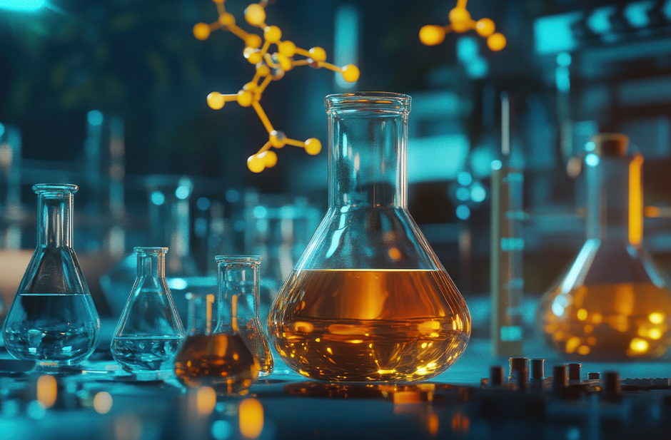
At PSE, we are dedicated to driving innovation and advancing research to address global challenges in green energy, new materials, climate change, and the environment.
We offer an inspiring academic environment where students learn from global experts, participate in cutting-edge research, and gain the skills needed to address global challenges in energy, environmental science, and materials sciences.
We invite students and researchers to follow the Dean’s Distinguished Lectures, a series of talks featuring internationally acclaimed scholars and professors from top universities worldwide.
13 December, 2024
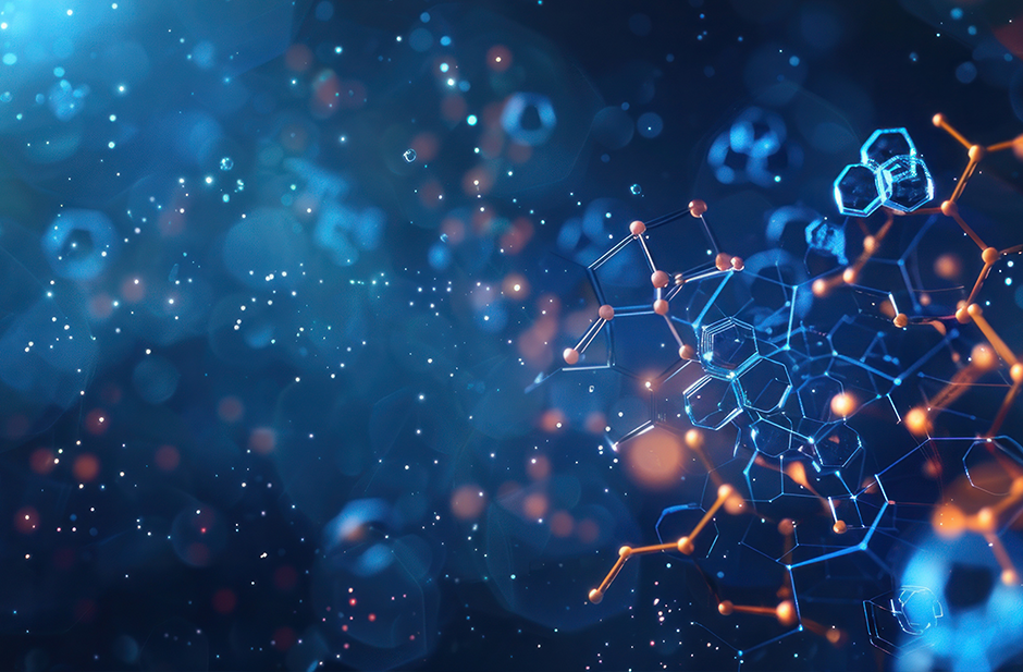
Hexagons of hexagonal boron nitride join up to form two-dimensional insulator for next-generation electronic devices.
A method that can grow a useful insulating material into exceptionally high-quality films that are just one atom thick and is suitable for industrial-scale production has been developed by an international team led by Xixiang Zhang from KAUST.
The material, called hexagonal boron nitride (hBN), is used in semiconductor devices and can also enhance the performance of other two-dimensional (2D) materials such as graphene and transition metal dichalcogenides (TMDs).
Researchers can combine 2D materials to build tiny electronic components for quantum computing, electronic communications and other applications. While most 2D materials conduct electricity, hBN is one of the few that is an insulator, making it an indispensable component within many of these devices.
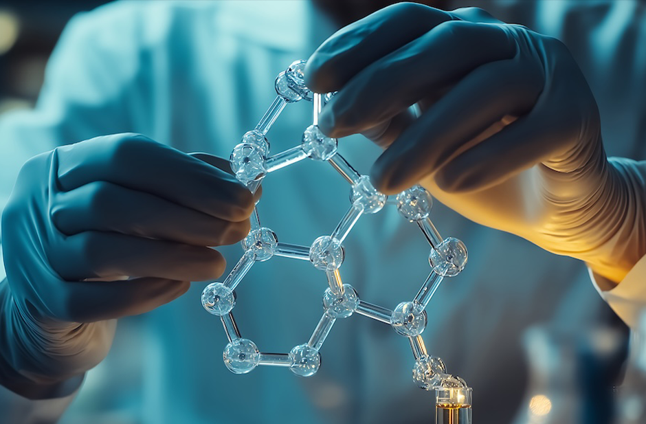
In the laboratory, hBN flakes are often peeled from bulk samples of the material, a time-consuming and size-limiting approach that is unsuitable for mass manufacturing. Alternatively, an industrial process called chemical vapor deposition (CVD) can produce hBN by decomposing a precursor called ammonia borane. Boron and nitrogen atoms released from the precursor then form triangular islands of hBN on a copper foil, and these islands gradually grow larger until they join together into a continuous honeycomb lattice.
The team has improved this process by growing hBN from hexagonal islands instead, producing a higher-quality film. “Hexagonal islands have fewer defects, making the final film more uniform and reliable,” says Zhang. The method depends on adding a trace of oxygen during the growth process.
Read more at KAUST Discovery.
Feb 2026
Mechanical Engineering Seminar
Static electricity whispers its secrets through a microscopic mechanical contactFeb 2026
Earth Systems Science and Engineering Seminar
Recent Micropaleontological Highlights from Saudi ArabiaFeb 2026
Dean's Distinguished Speaker Seminar
My quantum dot journey: from water to infrared, and finally to luminescent saltsIn PSE, we advance scientific discovery and innovation through interdisciplinary collaboration, addressing global challenges with impactful research. Join us in shaping a sustainable future through excellence in science and technology.