Jun 2025

Ph.D. Dissertation Defense Committee
Abstract:
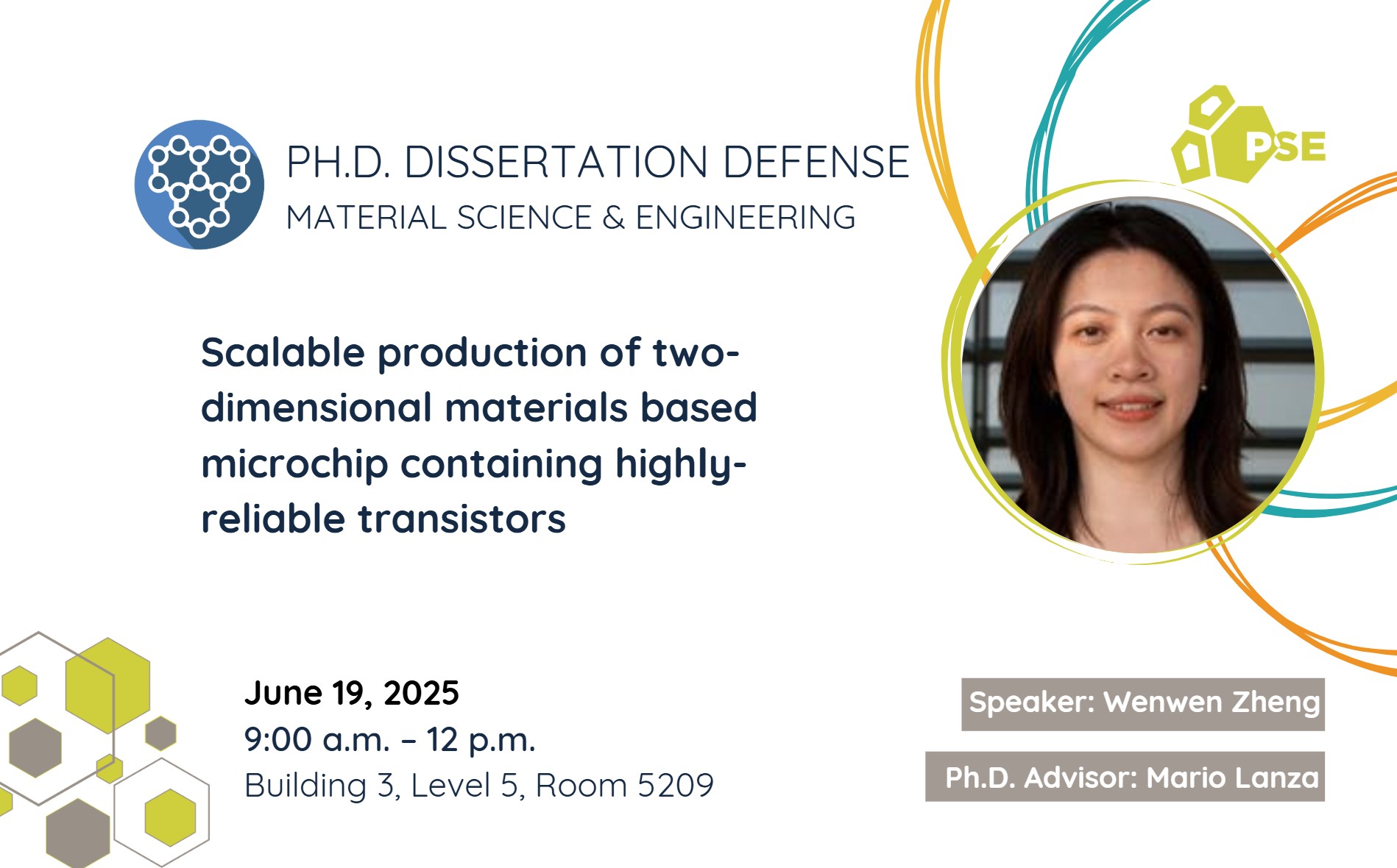
The integration of two-dimensional (2D) materials into electronic devices offers a promising path for advancing beyond-silicon technologies. However, challenges such as defect formation during metal deposition, poor electrode adhesion, and limited scalability hinder reliable device fabrication. This dissertation addresses these issues through fundamental studies and scalable fabrication strategies, culminating in the development of highly reliable graphene-based microchips.
First, the origins of metal-induced defects on 2D materials are investigated. It is shown that metal evaporation under moderate vacuum (5 × 10⁻⁶ Torr) enables defect-free van der Waals interfaces. Cross-sectional transmission electron microscopy (TEM) and density functional theory (DFT) simulations reveal that surface water weakens covalent bonds, promoting defect formation. This insight offers a clear pathway to defect mitigation, critical for high-performance 2D devices.
Building on this understanding, a novel photolithography protocol is developed using a negative photoresist to achieve partial coverage of the 2D material, followed by metal deposition under moderate vacuum conditions. This approach enables the formation of clean, damage-free metal/2D material van der Waals interfaces, significantly enhancing device performance. Most notably, the method achieves 100% fabrication yield, effectively overcoming long-standing adhesion and reliability challenges in 2D device manufacturing. This high-yield process marks a critical step toward scalable, industrial-grade production of 2D material-based electronics.
Finally, these advances are translated into a scalable process for fabricating reliable graphene field-effect transistors (GFETs). By replacing conventional metal-oxide dielectrics with multilayer hexagonal boron nitride (hBN), GFETs exhibit ultra-low hysteresis (< 20 mV), minimal shifts in on-state current and charge neutrality point after 2100 biasing cycles, and excellent device uniformity. These devices are further integrated into functional circuits, such as frequency doublers, highlighting their potential for high-frequency and sensing applications.
In summary, this study bridges fundamental insights with practical fabrication approaches, addressing key barriers in defect control, metal integration, and device reliability. The findings provide a foundation for the scalable integration of 2D materials into next-generation electronics.