Jun 2025

Ph.D. Dissertation Defense Committee
Abstract:
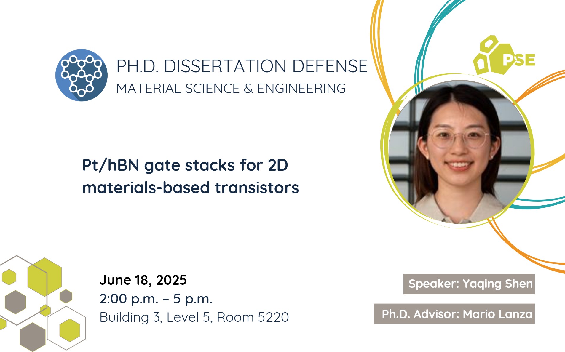
The semiconductor industry is striving to incorporate two-dimensional (2D) semiconducting materials as channel material into field-effect transistors (FETs) to sustain the progression of Moore's law. Traditional interfaces between 2D semiconductors and high-k dielectrics are typically fraught with traps that degrade device performance. Hexagonal boron nitride (h-BN) is a promising dielectric due to its ability to form nearly trap-free interfaces with 2D semiconductors. However, when produced using industry-compatible methods such as chemical vapor deposition (CVD), h-BN often suffers from native defects that increase tunnelling current and reduce dielectric strength. This study demonstrates that using metallic gate electrodes with high cohesive energy, such as platinum (Pt) and tungsten (W), significantly reduces the leakage current through CVD-grown h-BN by about 500 times in comparison to devices that utilize gold (Au) electrodes. Furthermore, these advanced h-BN/metal stacks achieve a high dielectric breakdown strength of a minimum of 25 MV/cm. The integration of 2D semiconducting materials as channels and 2D insulating materials as dielectrics enables the scaling down of 2D transistors to nanometre dimensions, potentially surpassing current limitations of Moore's law. This work thoroughly investigates the use of CVD h-BN as a gate insulator in 2D materials-based transistors, showing that high cohesive energy metals like Pt enhance dielectric strength and reduce leakage currents. The results indicate that transistors using CVD-grown h-BN and 2D materials for dielectrics and channels, respectively, exhibit robust performance and superior electrical properties, promising higher integration density in electronic circuits. Experiments on both microscale and nanoscale metal/h-BN/metal devices, multiple 2D transistors and a complementary metal-oxide-semiconductor (CMOS) microchip consistently support these conclusions. These findings present a viable path for advancing the performance and reliability of industrial 2D transistors.