
LATEST
NEWS
15 June, 2025
Detailed ‘movies’ that show how electrical charge flows through a layered material known as a 2D perovskite provide insights into how the perovskite could be fine-tuned to develop electronic devices that operate faster, last longer, and perform more efficiently.
“Researchers can use these results to carefully select the right number of layers and tailor surface chemistry to design improved 2D perovskite materials for applications such as solar cells and photodetectors,” says Lijie Wang from KAUST, part of the team behind the work.
Perovskites can form thin crystalline films that convert light into electricity or vice versa. They are being commercialized in next-generation solar panels and show promise in applications such as light-emitting diodes (LEDs). Researchers make perovskites by combining inorganic materials like lead iodide with carbon-based organic molecules. However, exposure to heat, moisture, or intense light can degrade perovskites and their performance.
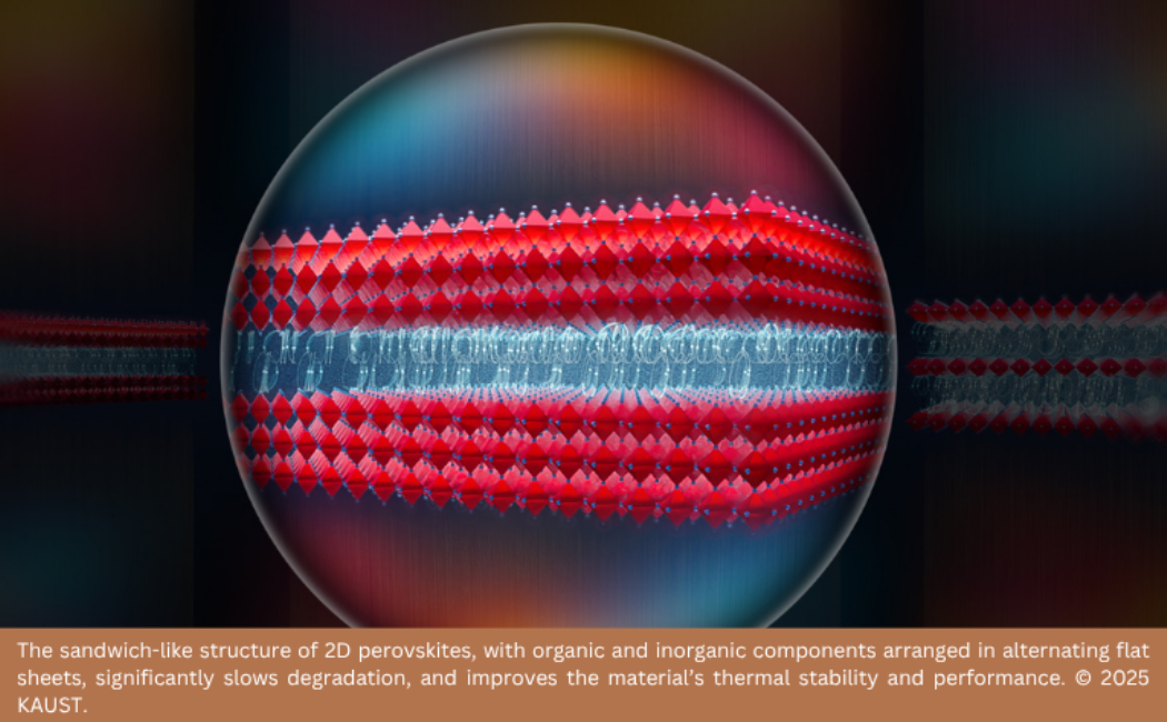
Researchers hope to solve these problems using closely related materials called 2D perovskites, in which the organic and inorganic components are arranged in alternating flat sheets, rather like a sandwich. The organic molecules serve as a barrier, preventing moisture and oxygen from reaching the inorganic slabs between them. “This structure significantly slows down the degradation processes and improves thermal stability,” says KAUST’s Omar Mohammed, who led the team.
Read more at KAUST Discovery.