An instrument error can lead to complete misidentification of certain crystals, reports a KAUST study that suggests researchers need to exercise caution when using electron microscopes to probe two-dimensional (2D) semiconductors.
2D transition metal dichalcogenides (TMDs) are being tapped for new electronic devices because they can exist in several crystal phases with properties ranging from semiconducting to metallic. Researchers use multiple tools to unravel the structure-property relationships in different TMD phases, but one of the most critical is the scanning transmission electron microscope. This instrument is capable of both resolving atoms on surfaces and chemically identifying them using variations in image contrast.
Areej Aljarb, a materials scientist working in Vincent Tung’s group at KAUST, was recently characterizing TMDs made from molybdenum disulfide (MoS2) when she spotted something troubling. Although initial spectroscopic analysis showed that she had produced semiconducting 2D films, the transmission electron microscope images indicated that MoS2 had arranged into a metallic crystal phase.
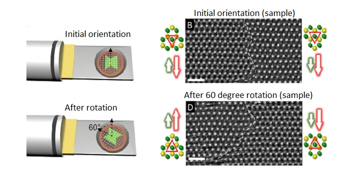
To resolve this difference, the team enlisted the help of Sergei Lopatin, an expert in microscopy. Together, they noticed that the electron beams emanating from their state-of-the-art instruments had unusual intensity patterns when they contacted the TMD surface. Instead of the expected spherical shapes, the beam’s intensity profiles appeared triangular. "This was clear evidence of an image-focusing problem known as astigmatism," notes Lopatin.

The relative position of the sample supported on TEM holder before (top) and after (bottom) rotation (left).The corresponding HR-STEM ADF images before (top) and after (bottom) an in-plane rotation by 60 degrees (right).
Reproduced under a Creative Commons license from reference one © 2020 KAUST
The lenses used to focus electron microscope beams always contain small imperfections that can blur images, especially at atomic-scale resolutions. The team realized that the observed astigmatic effects might impact the contrast of atoms appearing on the surface. By correlating computer simulations of the MoS2 surface with experimental microscopy, they saw several instances where crystal phases could be misidentified due to sulfur atoms changing appearance —and even disappearing—during imaging.
“Atomic contrast can be a powerful tool to deduce crystal phases, but these artifacts erode the foundations of such predictions,” says Tung. “It raises the possibility that there may have been many images already taken of 2D TMDs adversely affected by astigmatism.”
Experiments on other 2D surfaces, including graphene, confirmed that false phases can be observed in a range of materials. The researchers demonstrated that these effects could be mitigated by employing beams in which the electrons are nearly all energetically equivalent.
“Scanning transmission electron microscopy is invaluable in imaging the crystal structure of 2D materials; however, we need to be cognizant of imaging artifacts because ignoring them may lead to scientifically false claims,” says Aljarb.

