10 July, 2023
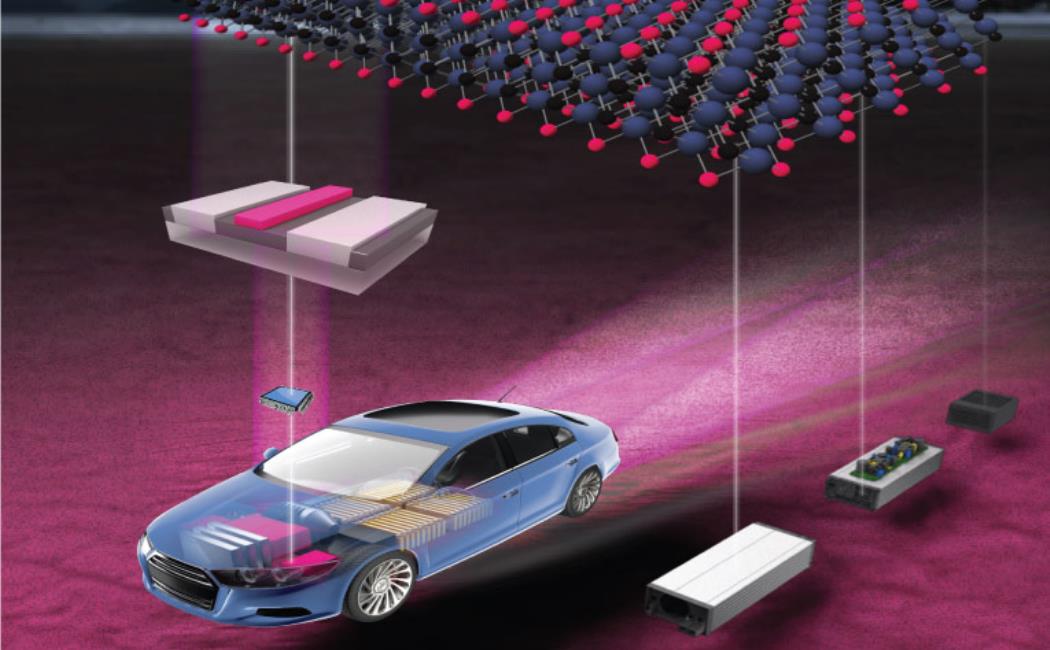
KAUST researchers have developed a two-dimensional MXene for semiconductor technology that could help to improve a range of high-power applications, including radar and satellite communications. © 2023 KAUST; Olga Kasimova.
Computers, despite all their apparent complexity, are basically just a large number of electronic switches, flicking on and off in the right order to process digital information. Semiconductor technology has made these switches very small and incredibly fast.
The semiconducting material gallium nitride holds promise to make them even faster. This is because the charge carriers in gallium nitride, such as electrons, can move through the material at high speed. This makes GaN useful in so-called high electron-mobility transistors, or HEMTs, for high-frequency and high-power applications, including mobile phone chargers, 5G base stations, radar and satellite communications.
A crucial aspect for optimizing the operation of a HEMT is making the electrical connection that switches the transistor on or off. These so-called Schottky gates can suffer from high leakage currents that flow even when the transistor is in its off state. This results in high power consumption and limits the voltage that can be applied before the device breaks down.
Chuanju Wang from Xiaohang Li’s team and Xiangming Xu from Husam Alshareef’s team, along with their co-workers and colleagues from India and China, have shown that these limitations can be minimized by fabricating the Schottky gate from a class of material known as MXenes: metallic two-dimensional atomically thin layers of transition metal carbides, nitrides or carbonitridesarticle " id="return-reference-1" href="https://discovery.kaust.edu.sa/en/article/21257/2d-metal-contacts-stop-transistor-leakage-currents-in-their-tracks/#reference-1">[1].
While conventional metals are the traditional choice for electrical contacts to GaN, chemical interactions between the two materials create defects that can trap electrical charge and significantly limit gate controllability. “The traditional metal gate contact materials have been deposited using methods such as electron-beam evaporation and sputtering, which have a direct chemical bond with the semiconductor substrate,” explains Wang.
Read more at KAUST Discovery.