31 May, 2023
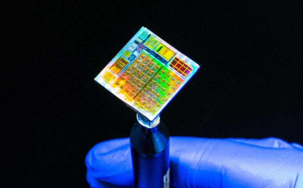
KAUST Professor Mario Lanza and his co-researchers have successfully designed the world's first 2D microchip using synthetic materials. © 2023 KAUST; Mario Lanza.
The first demonstration of a functional microchip integrating atomically thin two-dimensional materials with exotic properties heralds a new era of microelectronics.
The world’s first fully integrated and functional microchip based on exotic two-dimensional materials has been fabricated at KAUST. The breakthrough demonstrates the potential of 2D materials to expand the functionality and performance of microchip-based technologies.
Since the first fabrication of atomically thin layers of graphite — called graphene — in 2004, there has been intense interest in such materials for advanced and novel applications due to their exotic and promising physical properties. But, despite two decades of research, functional microdevices based on these 2D materials have proved elusive due to the challenges in fabricating and handling such fragile thin films.
Inspired by recent achievements in the Lanza’s lab on functional 2D films, the KAUST-led collaboration has now produced and demonstrated a prototype 2D-based microchiparticle " id="return-reference-1" href="https://discovery.kaust.edu.sa/en/article/21246/functional-2d-enabled-microchips-become-reality/#reference-1">[1]
“Our motivation was to increase the technology readiness level of 2D material-based electronic devices and circuits by using conventional silicon-based CMOS microcircuits as a base and standard semiconductor fabrication techniques,” says Lanza. “The challenge, however, is that synthetic 2D materials can contain local defects such as atomic impurities that can cause small devices to fail. Also, it is very difficult to integrate the 2D material into the microchip without damaging it.”
The research team optimized the design of the chip to make it easier to fabricate and minimize the effect of defects. They did this by fabricating standard complementary metal oxide semiconductor (CMOS) transistors on one side of the chip and feeding interconnects through to the underside, where the 2D material could be transferred reliably in small pads less than 0.25 micrometers across.
Read more at KAUST Discovery.