Nov 2026
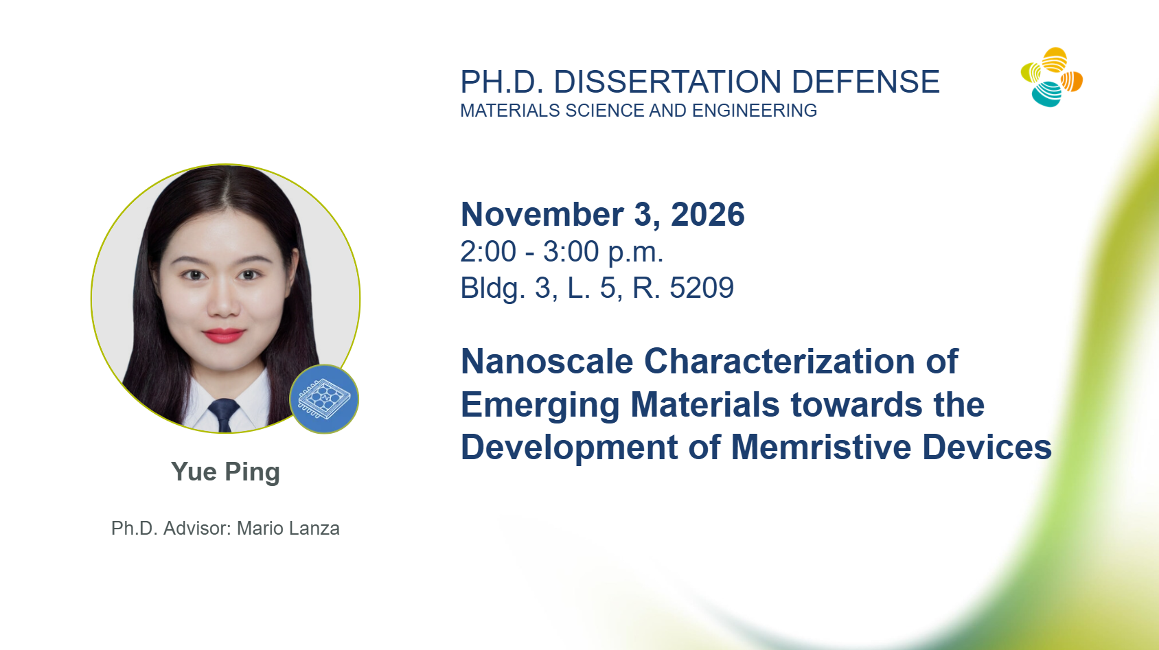
Nanoscale Characterization of Emerging Materials towards the Development of Memristive Devices
Ph.D. Dissertation Committee:
- Committee Chair: Prof. Nazek El-Atab
- Ph.D. Advisor: Prof. Mario Lanza
- External Examiner: Prof. Fei Hui
- Committee Member: Prof. Alfonso Caraveo
Abstract:
Two-dimensional (2D) materials and their heterostructures are widely regarded as key enablers for extending nanoelectronics beyond the physical limits of conventional silicon-based complementary metal-oxide-semiconductor (CMOS) technology. Realizing this potential, however, depends on the ability to characterize these materials at the nanoscale and to synthesize them with a quality and uniformity compatible with industrial device fabrication. This dissertation addresses both challenges, combining nanoscale electrical and structural characterization of emerging 2D materials with the scalable synthesis of hexagonal boron nitride (hBN) for nanoelectronic and memristive applications.
The first part of this work develops and applies atomic force microscopy (AFM)-based techniques to characterize two technologically relevant material systems. Ti3C2Tx MXene thin films were characterized to establish quantitative morphological and thickness statistics relevant to their use in energy storage and sensing devices, while conductive AFM (C-AFM) and scanning electron microscopy (SEM) were used to probe the nanoelectronic and morphological properties of perovskite solar modules, correlating local current behavior with device-level performance and degradation pathways.
The second part focuses on hBN, a wide-bandgap 2D insulator, whose dangling-bond-free van der Waals surface makes it an attractive gate dielectric and resistive switching medium. A wafer-scale production process for hBN on 200 mm wafers using closed coupled showerhead chemical vapor deposition was developed and evaluated. Structural and morphological characterization confirmed the crystalline quality of single-batch material, while statistical analysis across full wafers and multiple growth batches established the uniformity and reproducibility required for device integration. The resulting hBN films were successfully integrated as the gate dielectric in graphene field-effect transistors (GFETs), demonstrating their compatibility with active device fabrication.
Finally, this dissertation reports the synthesis of nanocrystalline boron nitride (nc-BN) by low-pressure chemical vapor deposition (LPCVD) and its integration into resistive switching memory devices. The devices exhibited reproducible switching between high- and low-resistance states, and the underlying conduction mechanisms were investigated to identify the limitations of the current device architecture and to propose pathways for improving switching performance, endurance, and reliability.
Together, these results advance the nanoscale understanding of emerging 2D materials and establish hBN and nc-BN as viable, scalable materials for next-generation nanoelectronic and memristive devices, bridging the gap between laboratory-scale materials discovery and industrially relevant device fabrication.